- 您现在的位置:买卖IC网 > Sheet目录1995 > DS4404N+ (Maxim Integrated Products)IC DAC 4CH I2C ADJ 14-TDFN
DS4402/DS4404
Two/Four-Channel, I2C Adjustable Current DAC
4
______________________________________________________________________
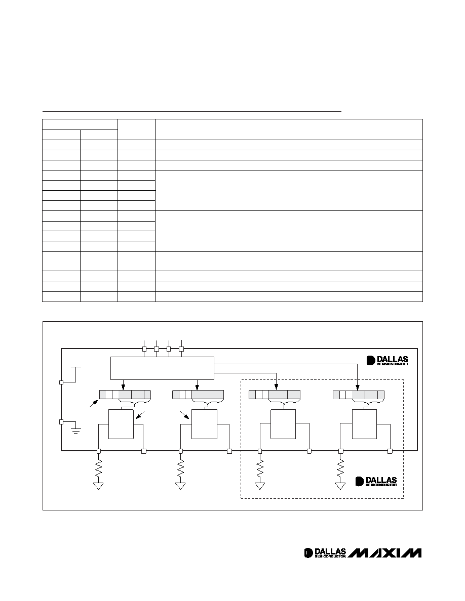
VCC
RFS0
RFS1
RFS2
RFS3
SDA SCL
A1
A0
GND
FS0
FS1
OUT1
OUT0
CURRENT
DAC0
F8h
F9h
SOURCE OR
SINK MODE
FS2
OUT2
FS3
OUT3
CURRENT
DAC3
31-POSITIONS
EACH FOR SINK
AND SOURCE
MODE
FAh
FBh
DS4402/DS4404
DS4404
CURRENT
DAC1
CURRENT
DAC2
I2C-COMPATIBLE
SERIAL INTERFACE
Figure 1. Functional Diagram
Pin Description
PIN
DS4404
DS4402
NAME
FUNCTION
1
SDA
I2C Serial Data. Input/output for I2C data.
2
SCL
I2C Serial Clock. Input for I2C clock.
3
GND
Ground
4
—
FS3
5
—
FS2
6
FS1
7
FS0
Full-Scale Calibration Input. A resistor to ground on these pins determines the full-scale
current for each output. FS0 controls OUT0, FS1 controls OUT1, etc. (DS4402 has only
two inputs: FS0 and FS1.)
8
OUT0
10
OUT1
12
—
OUT2
14
—
OUT3
Current Output. Sinks or sources the current determined by the I2C interface and the
resistance connected to FSx. (DS4402 has only two outputs: OUT0 and OUT1.)
9, 11
A0, A1
Address Select Inputs. Tri-level inputs (VCC, GND, N.C.) determine the I2C slave address.
See the Detailed Description section for the nine available device addresses.
13
VCC
Power Supply
—
4, 5, 12, 14
N.C.
No Connection
—
EP
Exposed Pad. Leave unconnected or connect to GND.
发布紧急采购,3分钟左右您将得到回复。
相关PDF资料
DS4412U+
IC DAC DUAL CH I2C ADJ 8-USOP
DS4424N+
IC DAC 7BIT 4CH 5.5V 14-TDFN
DS4425BN+
IC OSC CLOCK 425MHZ 10-LCCC
DS4426T+T&R
IC DAC I2C-MARGINING 4CH 28-TQFN
DS4432U+
IC DAC 7BIT 2CH 5.5V 8-MSOP
DS4625P+150/200
IC OSC CLOCK 200MHZ 10-LCCC
DS4M133D+33
IC OSC CLOCK 133.33MHZ 10-LCCC
DS8005-RRX+
SMART CARD AFE DUAL 28SOIC
相关代理商/技术参数
DS4404N+T&R
制造商:Maxim Integrated Products 功能描述:DAC 4-CH CURRENT STEERING 5-BIT 14TDFN EP - Tape and Reel 制造商:Maxim Integrated Products 功能描述:I2C ADJUSTABLE CURRENT DAC 制造商:Maxim Integrated Products 功能描述:IC DAC 4CH I2C ADJ 14-TDFN
DS4404N+T&R
功能描述:数模转换器- DAC 4 Ch Adjustable RoHS:否 制造商:Texas Instruments 转换器数量:1 DAC 输出端数量:1 转换速率:2 MSPs 分辨率:16 bit 接口类型:QSPI, SPI, Serial (3-Wire, Microwire) 稳定时间:1 us 最大工作温度:+ 85 C 安装风格:SMD/SMT 封装 / 箱体:SOIC-14 封装:Tube
DS4404N+TR
制造商:MAXIM 制造商全称:Maxim Integrated Products 功能描述:Two/Four-Channel, I2C Adjustable Current DAC
DS4404NR
制造商:DALLAS 制造商全称:Dallas Semiconductor 功能描述:Two/Four-Channel, I2C Adjustable Current DAC
DS4404NT
制造商:DALLAS 制造商全称:Dallas Semiconductor 功能描述:Two/Four-Channel, I2C Adjustable Current DAC
DS4405MP00K
制造商:Thomas & Betts 功能描述:400A,PLG,3P4W,MG,3P440V,CC
DS4407MP000
制造商:Thomas & Betts 功能描述:400A,PLG,3P4W,MG,407,3P250V
DS4407MP00K
制造商:Thomas & Betts 功能描述:400A,PLG,3P4W,MG,00K,3P250V